Oh boy, this Data Recovery job was something else. It was a Samsung S21 Ultra that had extreme water damage. Waaaaay beyond trying to repair it to get data...
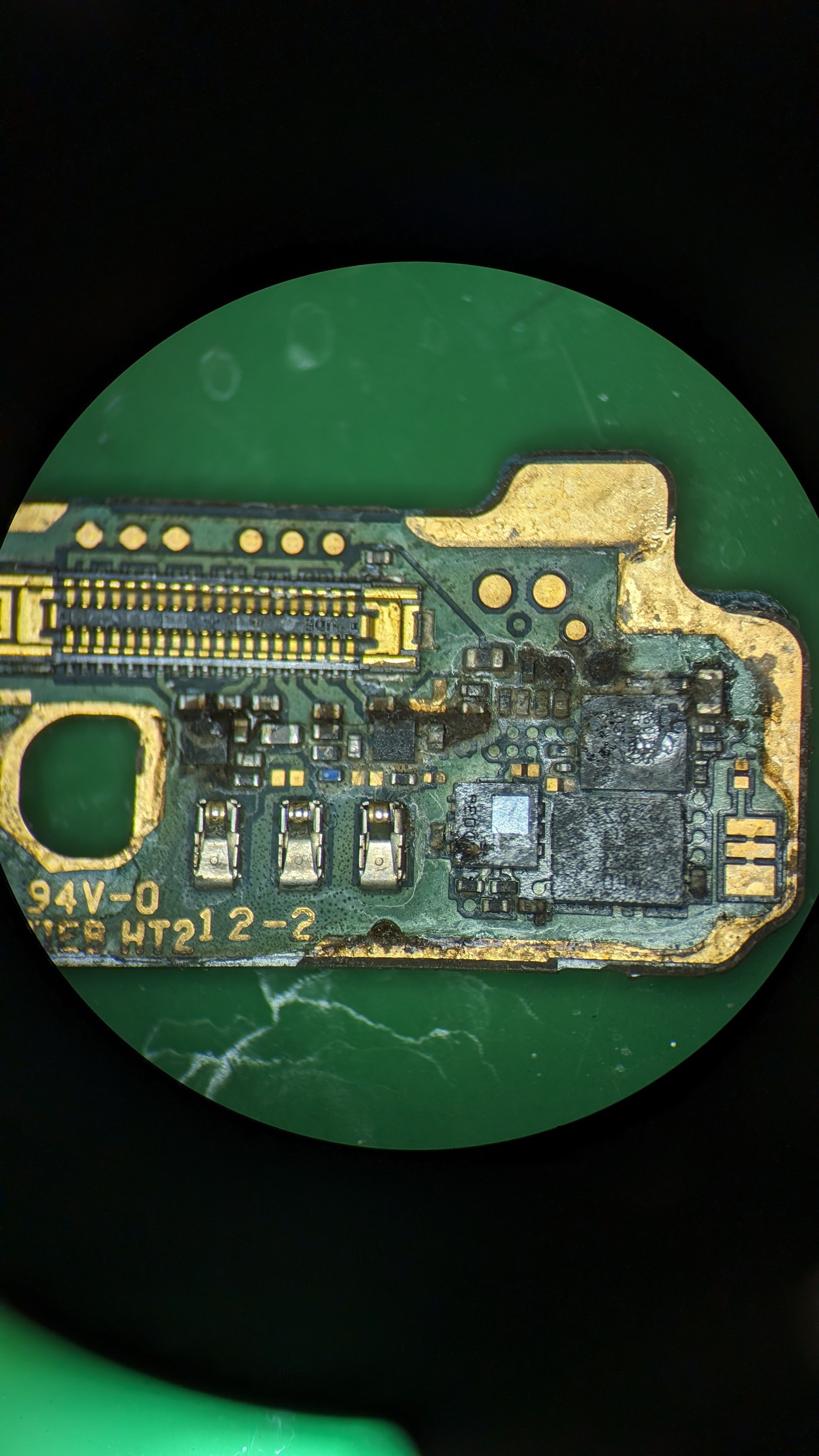
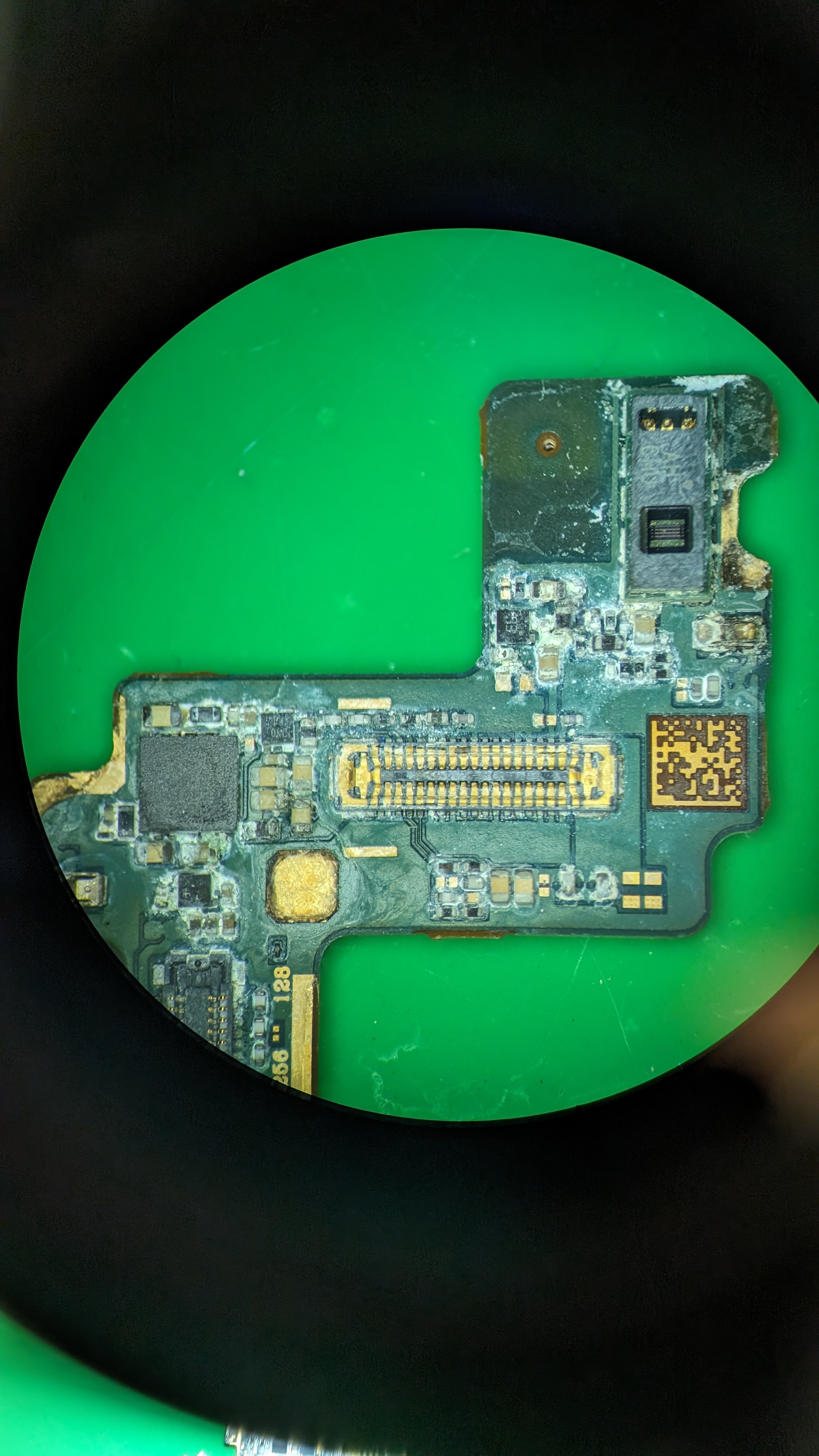
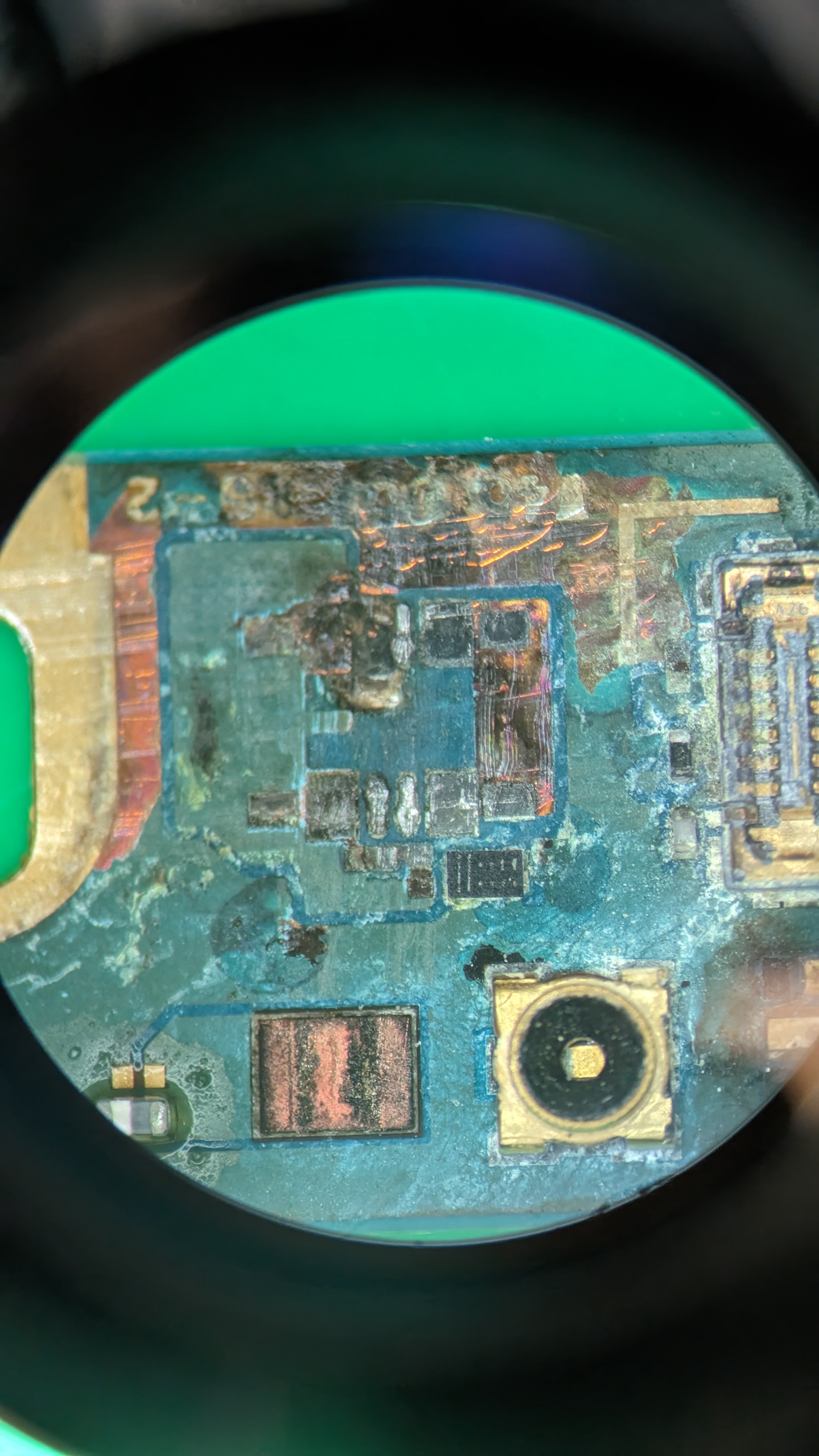
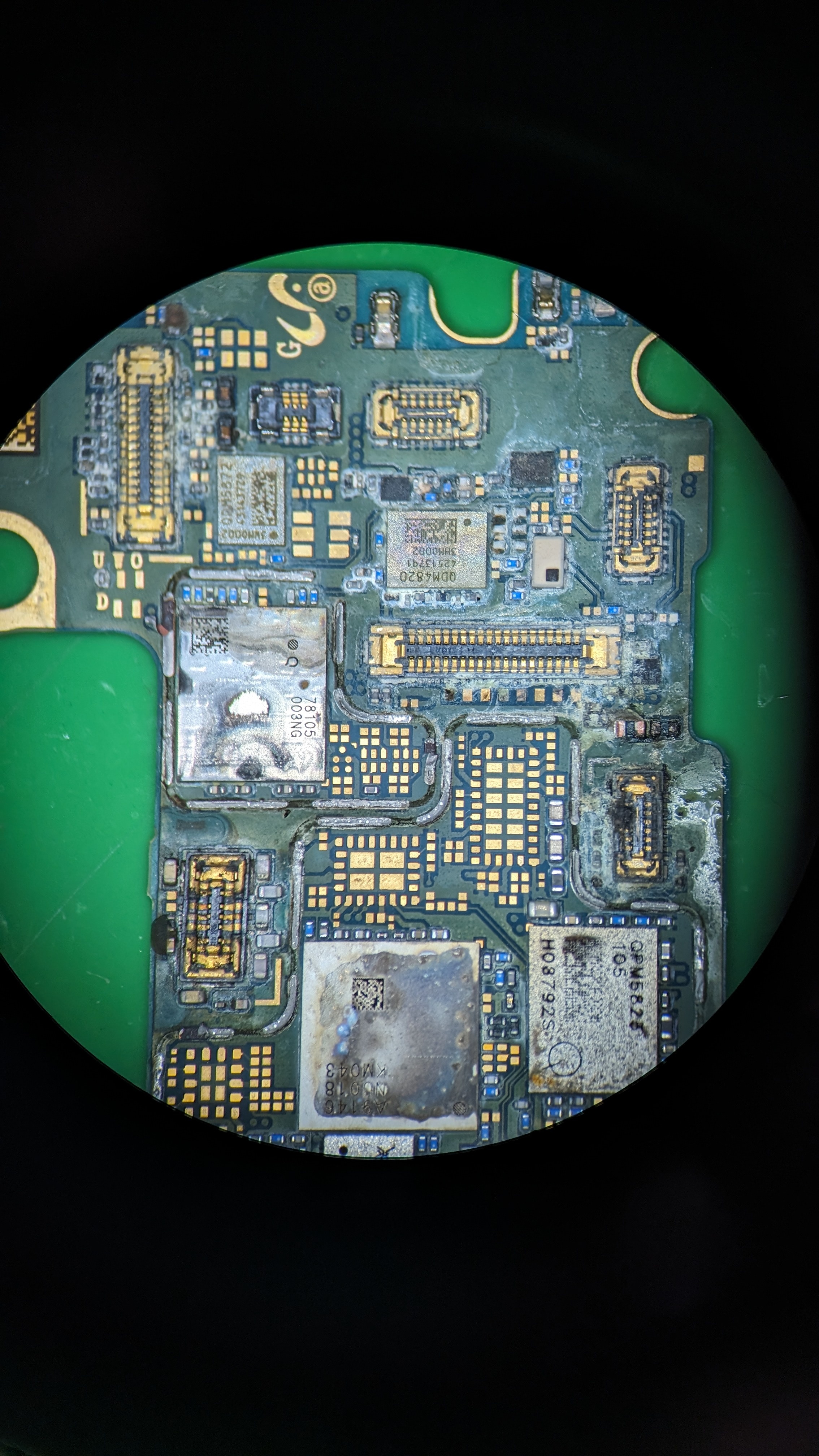
➡Swipe through all the pictures to get an idea of what we were working with.
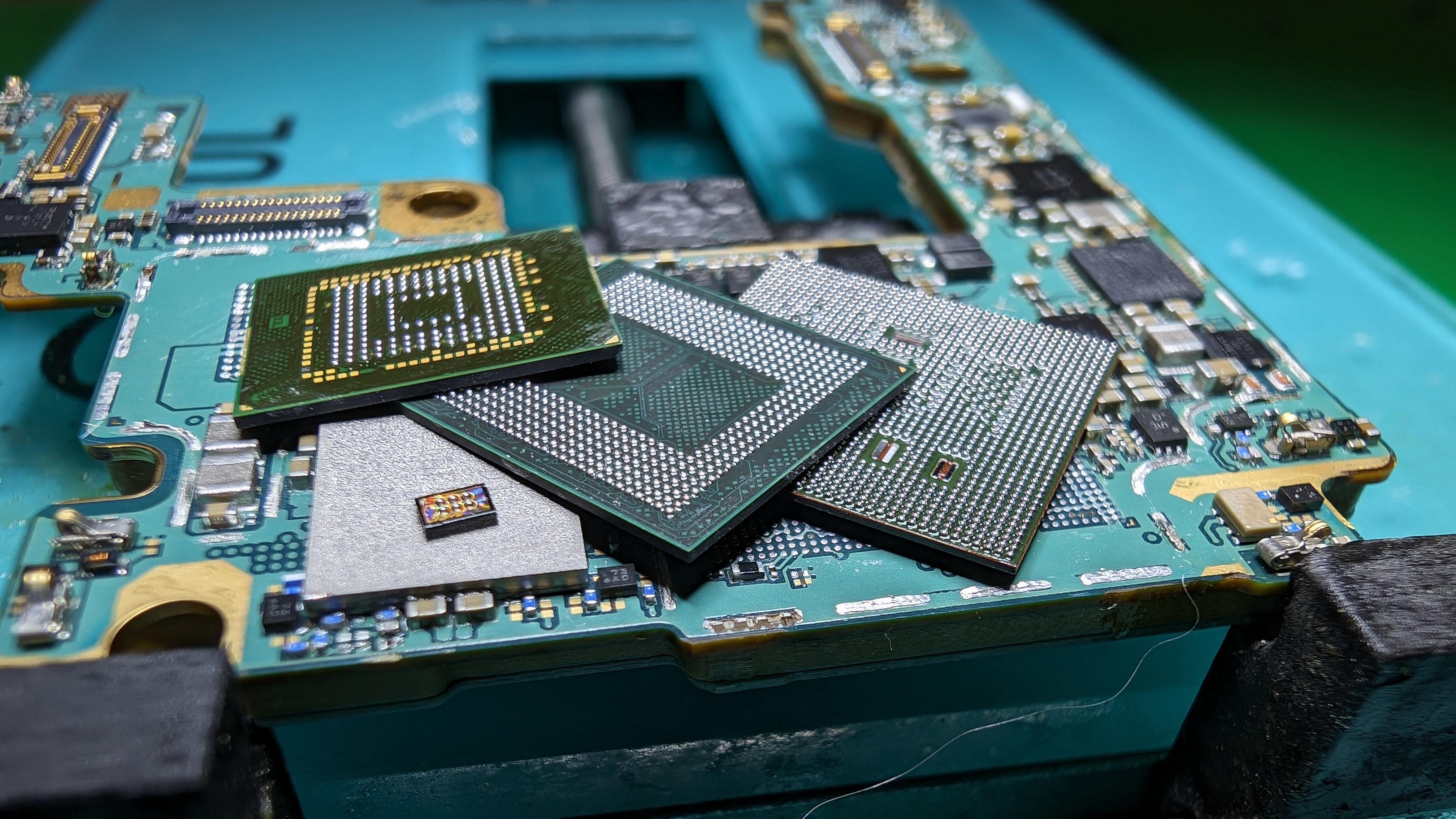
The only option here was a CPU Swap. If you saw my previous post, S21 models (and newer) have a "pin code IC" so to speak, that you must also transplant.
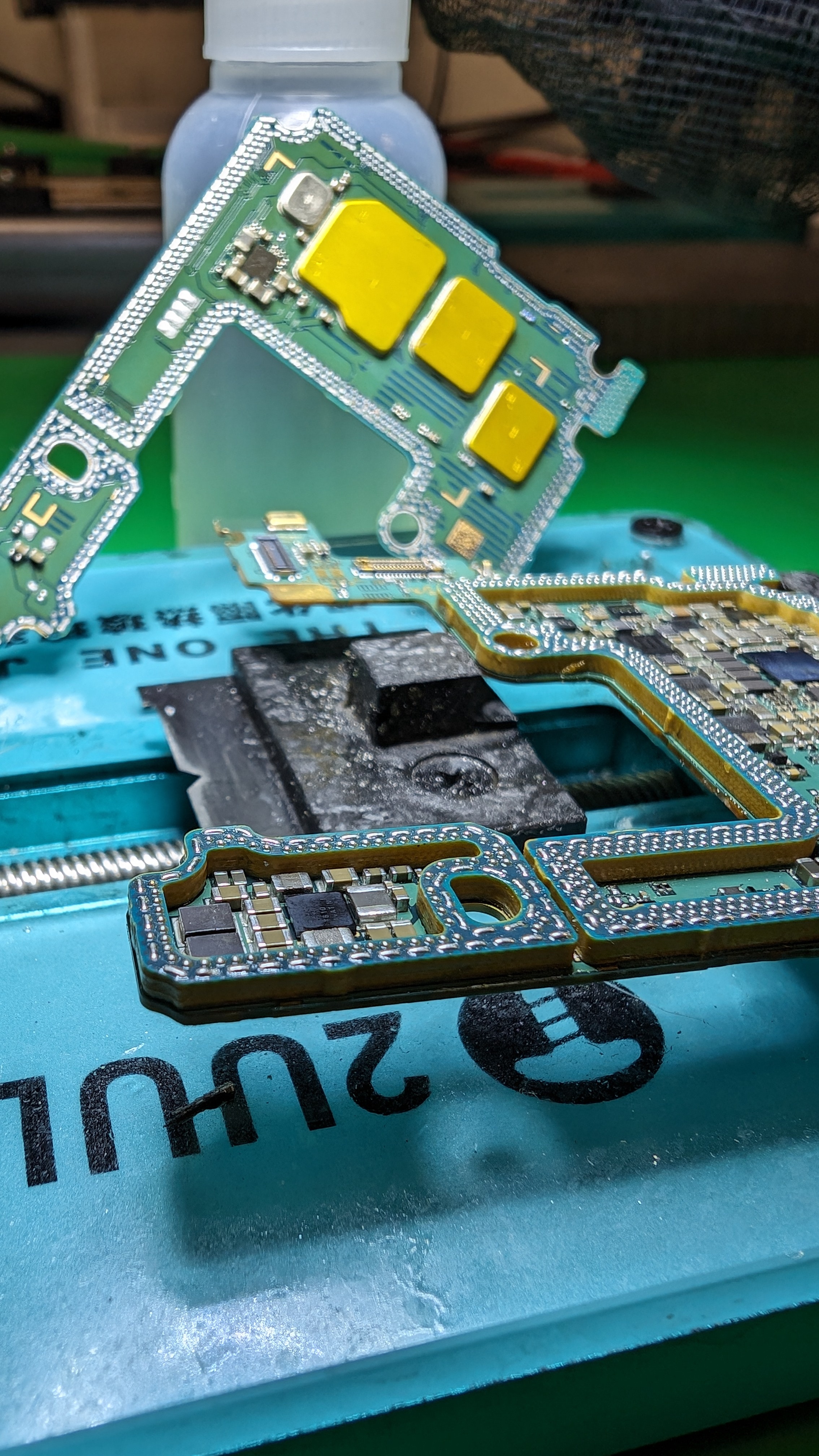
The problem is... on S21 series, this IC is inside the Samsung sandwich board. Which is a nightmare to split and even more difficult to reball.
My first step was to complete the CPU Swap to the donor board to make sure the phone can boot to begin with, which I was successful, but it wouldn't accept the correct pin code.
But at least I know the CPU and UFS are good and didn't die from all the water damage. And this confirms the donor is good & the parts I have are good.
Then I went for the split both donor & customer's board. I also made a video of this process on a previous post, so if you didn't see it, go check it out on my page.
Easily swapped the small 6 legged IC inside the sandwich, so I can get the pin code to work
Wicked both top & bottom layers
And attempted to reball the sandwich & this is where my troubles began. At first, we go No Power... WHOOPS
Checking on DCPS, I can see some heat on the side of the board.
I split the sandwich again & noticed some solder balls looked uneven. Maybe they bridged when I tried to sandwich. No shorts on top board & none detected on bottom board.
I tried re-squishing the sandwich without reballing and we got some life! BUT the image was all distorted. It was all static. I diode mode the connector & cross referenced ZXW and noticed some pins were reading as ground.
Those pins were not ground on the customer's board and of course, they go through the interposer.
So there I am, splitting this sandwich again.
I check those pads on the interposer & the short is gone. So it was definitely bridged.
I try to reball the sandwich again and viola! We got image, but charging was a little weird... then I see it's just bootlooping. It was only stuck at the first Samsung logo. I also noticed it would auto boot when plugging it into the charger. Samsungs do not auto boot, like iPhones.
So all this told me, there's still a problem somewhere.
I tried splitting AGAIN, and just re-squishing.
Same thing
Reflowed it and same results.
I went back and just decided to reball the "pin code IC" one more time, then wick the top & bottom boards again and try to reball again.
I do it.... and it doesn't charge. It doesn't even turn on my meter 😭
But it does boot with the power button, but once again, it's bootlooping.
SMH
So then I checked the board & noticed there's a gap in the sandwich. I rehot the sandwich & gently press down in hopes to connect the solder joints from the top & bottom board, but also have to pray that no bridges occur.
I do it. Visually, it looks like the gap is still there, but I can see solder joints stretching across the 2 sides & making connection.
I reassemble & plug in the charger... the meter lights up and the phone shows the lightning/charging symbol... then the temp warning. Of course, I didn't have the wireless charging coil plugged in. I plug it in & try again.... and we get the charging symbol.
AND it doesn't auto boot like before. This is an interesting change of events.
I use the power button to boot
It stays at Samsung logo for what feels like an eternity!
AND THEN WE GET THE LOCK SCREEN!
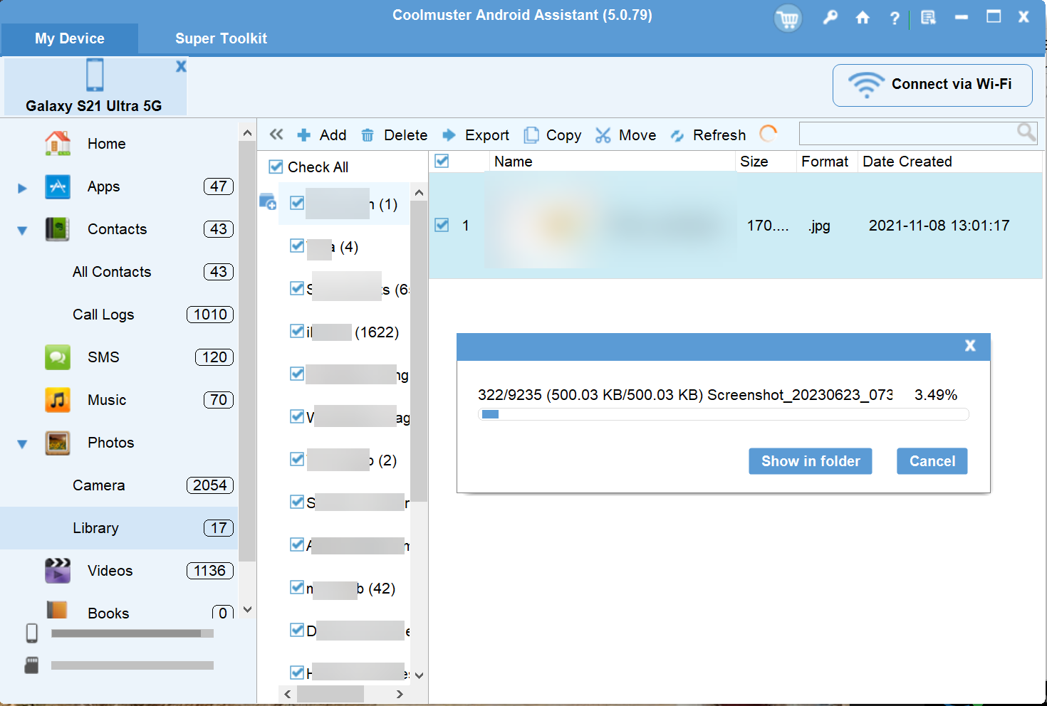
I type in the pin code.. BOOM! It unlocked
And here I am, typing out this story before I forget it all, while I download about 97GB of pics, videos, contacts, texts using CoolMuster.
YES, I know this was a long story, but here you are, reading it. So thanks for joining me in this journey, kind of, since you weren't really here.
How many Samsung sandwich boards have you reballed in your life?
If you have a Seek Thermal Cam, you're missing out if you don't have a VCC Seek Stand: https://www.vccboardrepairs.com/buy-seek-stand
Injured Gadgets just got these back in stock, so get them while you can!
It can take us a while to build these out sometimes, so they're sometimes out of stock for a while, but we're working towards always having inventory ready to build more as they sell out.
This stand makes using a thermal cam so easy. So much better than any other thermal solution on the market.
It allows you to get real close up (using my Macro Lens), and easily find where the short is coming from.
Plus it's hard free, so you can have your hands free to try to boot the device from DCPS, while having an image that is in focus & not moving around.
You can even record a video through the app, while you inject voltage into the short, so you can go back & see exactly which component was it that was heating up.
Save yourself lots of time by getting a Seek Cam, Stand & Macro Lens! ...
Anyone who is doing game console repairs, knows how many screws you need to remove to access the motherboard.
Especially the PS5, with the 5,000 screws or so.
If you don't already have an electric screwdriver, GET ONE ASAP.
🌟 Cordless Screwdriver with T9 Bit: https://amzn.to/3E5duCj
🌟Extended T9 Bit: https://amzn.to/3c4YJac
It's rechargeable through micro USB and allows you to easily swap the tips out. You can also fold it to be straight or L shape.
Let me know below if you are already using an electric screwdriver 👇👇
In case you haven't heard, I will be moving from Las Vegas, NV to Star, ID.
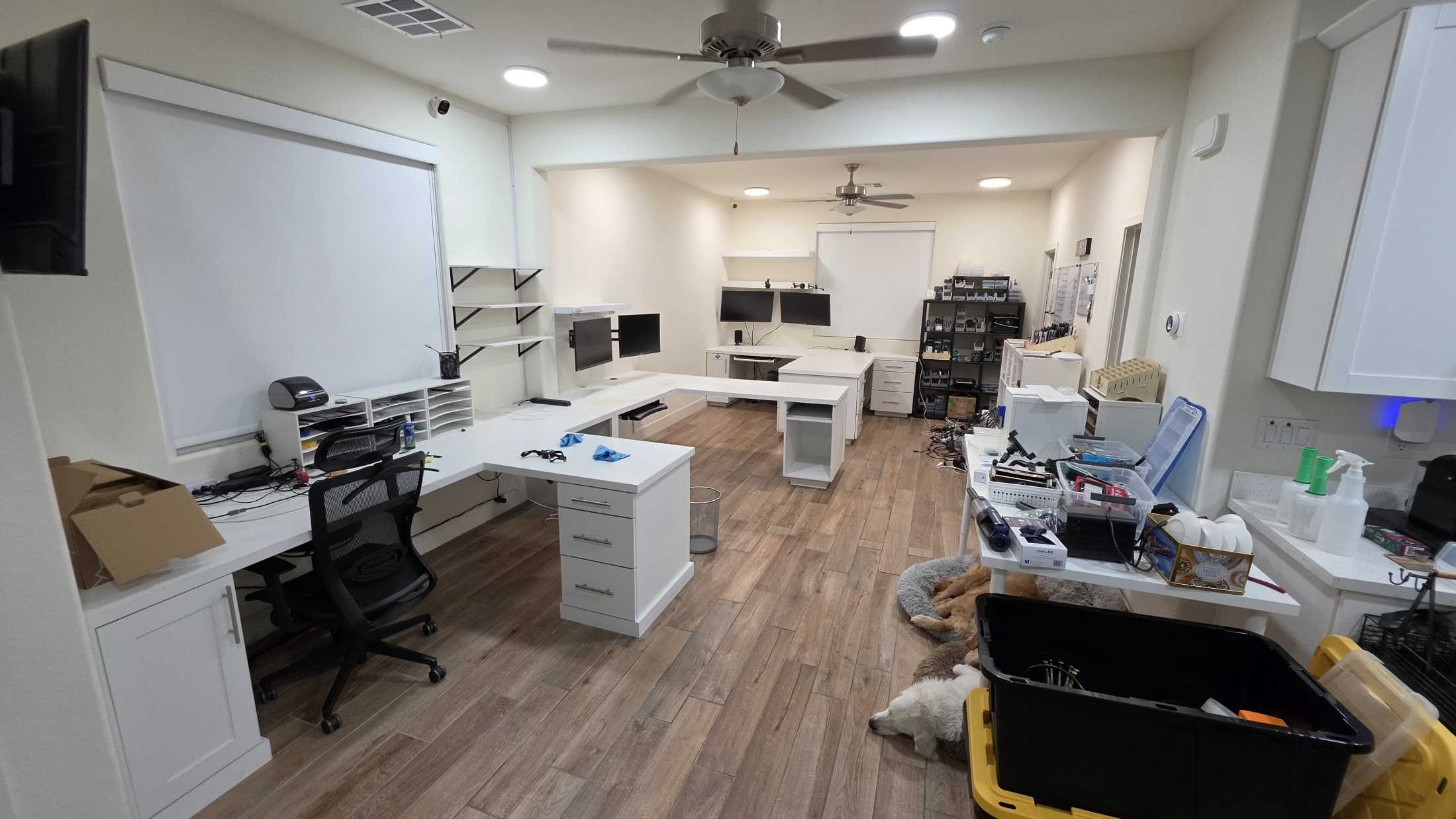
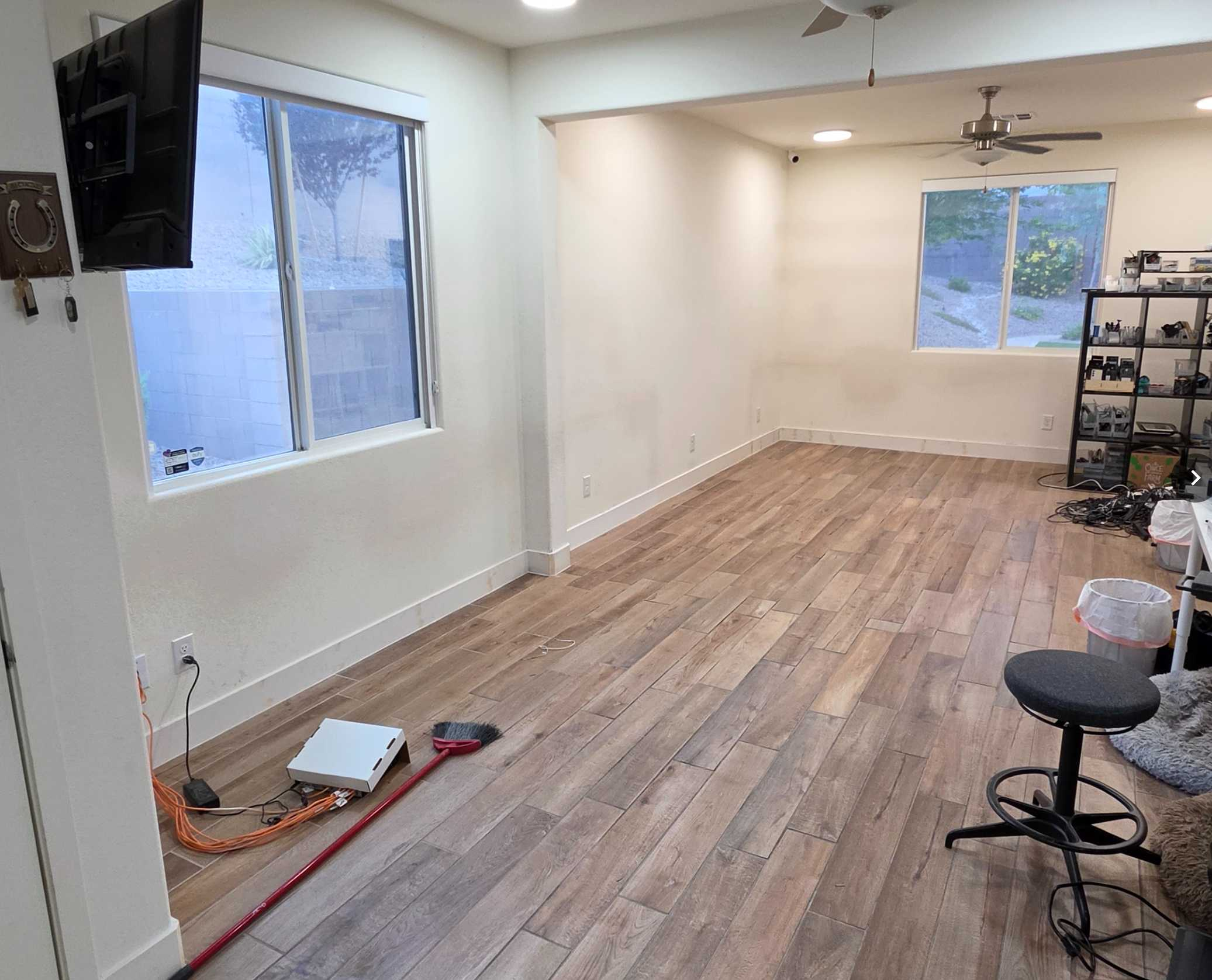
In my Las Vegas office, I had fully custom built workbenches for myself & my employee(s). But now it's time to go & tear everything down.
I'm really sad since these benches felt like the perfect layout! Or maybe I just got used to them.
I've attached some pics of what it looked like before & now that's all gone.
I do have some good news tho.... I recorded a detailed video of my office for youtube! I'll be posting that video soon!
Like this post if you want to see that video!
Hey guys! I'm so glad to finally get here. Thank you Jesse for the encouragement. Took me a minute but I'm here. I'm so eager to learn and grow. I have some experience with soldering etc, I can treat with obvious issues but there's something about diagnosing issues (especially with iPhones) that I have trouble with. I'm hoping this community can help with that.
Currently I have two iPhone 13 devices that need repair. One is stuck in recovery mode. A flash was attempted but there was an error during the process (Error 4013).
The other 13 does not boot or charge. It pulls 0.02A on the ammeter and I can feel both the back getting really hot. I tried this with two batteries. I also noticed that the wireless charging IC also gets very hot (338S00817) even when using a wired charger.
Remember I'm a noob so please....be gentle. Any help greatly appreciated. Thanks in advance!
A funny example of why board repair are still very human skills.
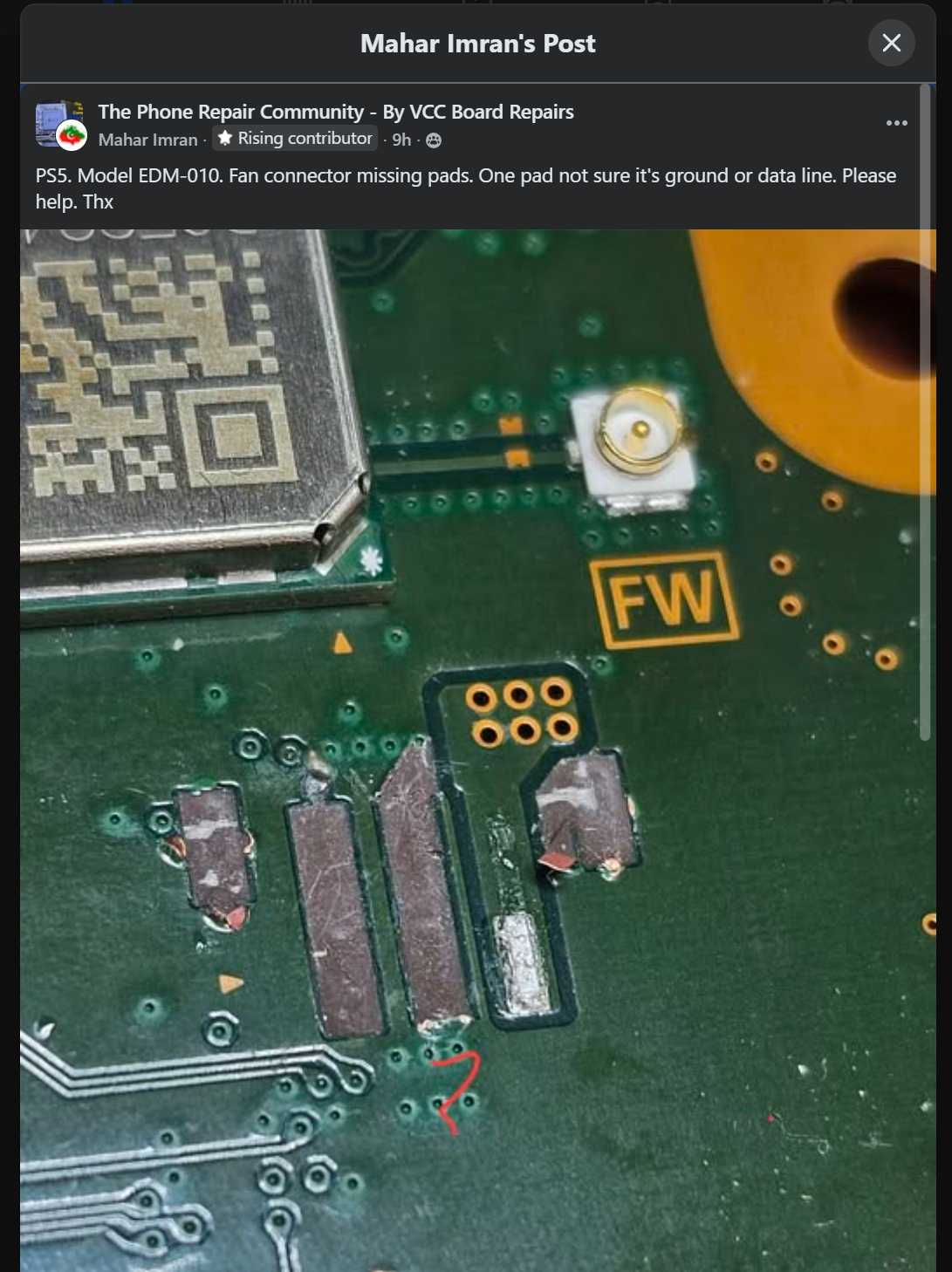
Someone posted in my Facebook group asking for help identifying a ripped pad on a PS5 fan connector. The connector had been torn off the board, and they wanted to know what signal the missing middle pad belonged to so they could run a jumper.
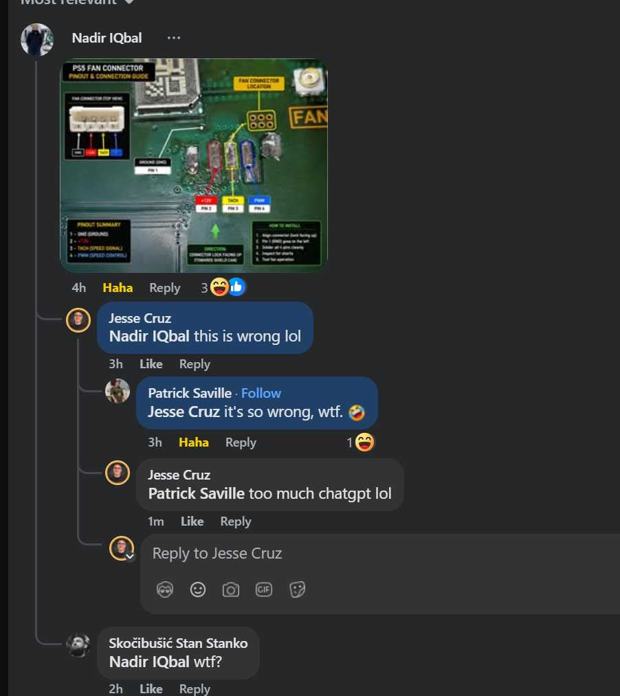
A commenter decided to let AI handle it.
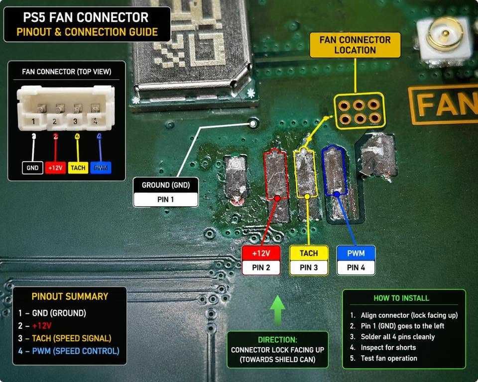
They fed the photo into ChatGPT and got back a nice-looking annotated diagram showing all the pin functions. The problem?
It was completely wrong.
The AI labeled the missing pad as the TACH signal when in reality that pad is ground.
The scary part is that if you didn't already know the answer, the diagram looks convincing. It has arrows, labels, colors, callouts, and all the confidence in the world. Yet it still gave bad information that could send someone down the wrong path.
This is one of the reasons I don't lose sleep over AI replacing board repair technicians.
AI is incredibly good at summarizing information that already exists publicly. But in...